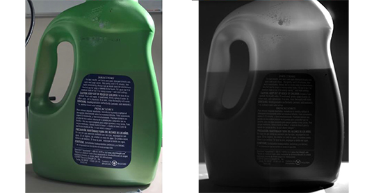
Infrared imaging, as a complement to imaging in the visible range (400-780 nm), offers new possibilities in many fields of application. For example, certain materials are opaque in the visible or paint deposits interfere with reliable assessment of product quality. Infrared imaging enables further insights in many cases.

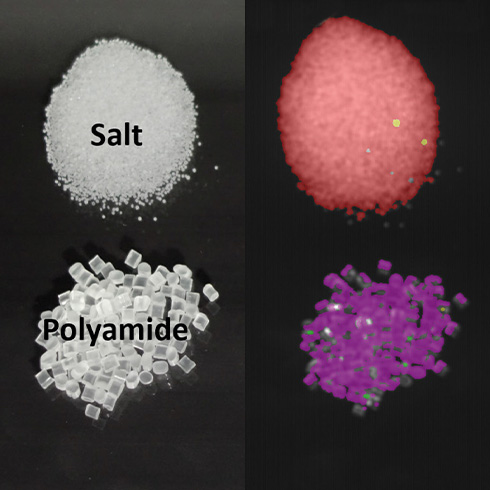
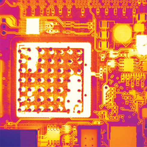
Near- and short-wave infrared (NIR/SWIR) is used, among other things, for silicon inspection in semiconductor or solar cell production. Here, the Si substrate becomes transparent and thus possible impurities and defects can be detected. The mid- and long-wavelength (MWIR/LWIR) infrared range, due to direct molecular absorption or thermal differences, makes small gas and liquid leaks visible, for example, or uses thermal imaging to reveal faults and weakness in mechanical or electrical systems. Chemical imaging allows to distinguish similar looking materials by their molecular composition.


